 Normal Supply
14-channel output, configurable as HSTL or LVDS
Maximum output frequency
6-channel output up to 1.25 GHz
8-channel output up to 1 GHz
Depends on the frequency accuracy of the voltage-controlled crystal oscillator (VCXO) (start-up frequency accuracy: <±100 ppm)
Each output provides a dedicated 8-bit divider
Coarse delay: 63 steps, each step being half the output frequency of the RF VCO divider, unaffected by jitter
Fine delay: 15 steps, resolution of 31 ps
Typical output skew: 20 ps
Duty cycle correction for odd divider settings
Output 12 and Output 13, VCO output at power-on
Absolute output jitter: <160 fS (at 122.88 MHz)
12 kHz to 20 MHz integration range
Digital lock-in frequency detection
SPI and I2C compatible serial control ports
Dual PLL architecture
PLL1
Using an external VCXO to reset the reference input clock
Phase detector rate: up to 110 MHz
Redundant reference input
Automatic and manual reference switching modes
Recovery and non-recovery switching
Keep mode supports reference loss detection
The low-noise LVDS/HSTL output provided by the VCXO can be used for RF/IF frequency synthesizers
PLL2
Phase comparator rate: Up to 275 MHz
Integrated low-noise VCO
Package: LFCSP-72 (10x10)
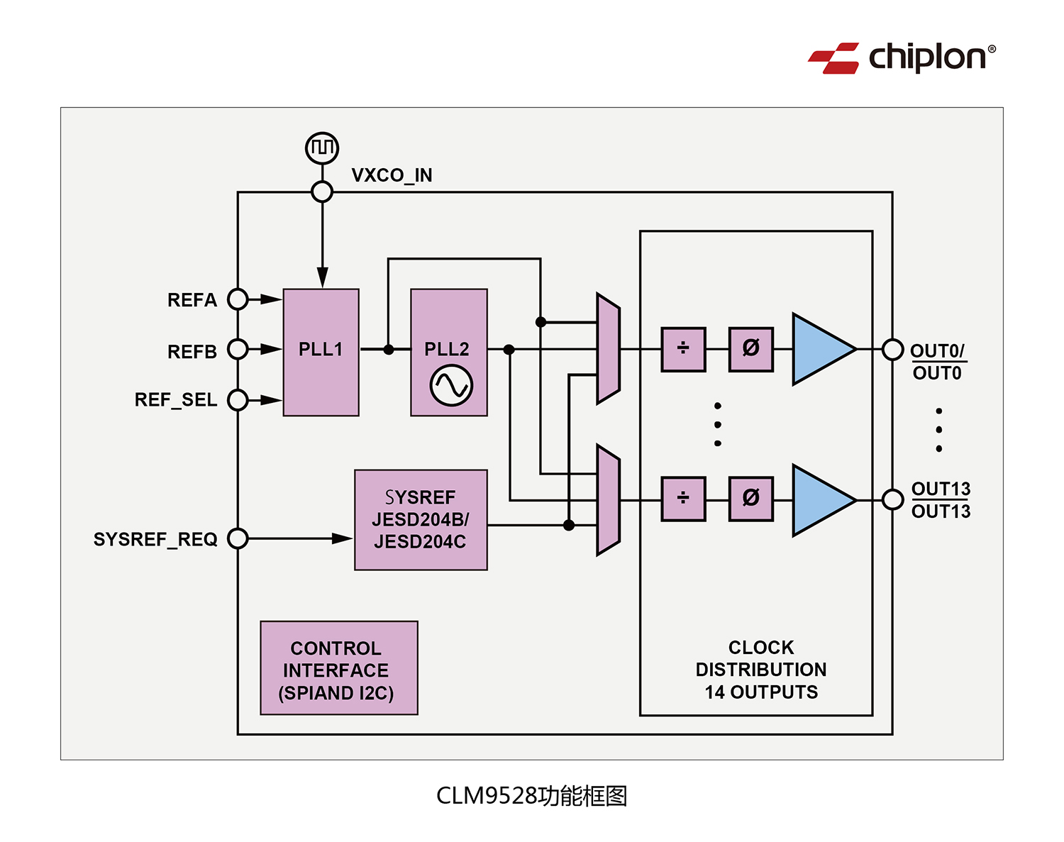
CLM9528 is a dual-stage phase-locked loop (PLL) developed with great dedication by Chiplon Microelectronics. The first-stage PLL reduces the jitter of the system clock to achieve the regulation of the input reference voltage. The second-stage PLL provides a high-frequency clock, enabling lower integral jitter and lower bandwidth noise from the clock output driver. The external VCXO supplies the low-noise reference voltage required by PLL2 to meet stringent phase noise and jitter requirements, achieving acceptable performance. The tuning frequency range of the on-chip VCO is from 3.450 GHz to 4.025 GHz. The integrated SYSREF generator outputs single-shot, N-shot or continuous signals and synchronizes with the outputs of PLL1 and PLL2 to align the times of multiple devices.The CLM9528 generates six-channel outputs with the highest frequency of 1.25 GHz (outputs 0 to output 3, output 12 and output 13), as well as eight-channel outputs with a maximum frequency of up to 1 GHz. Each output can be configured to directly come from PLL1, PLL2 or the internal SYSREF generator. Each of 14 output channels contains a divider with digital phase coarse adjustment functionality, as well as an analog fine phase delay module, allowing all 14 outputs to have high flexibility in timing alignment. The CLM9528 can also be used as a flexible dual-channel input buffer to achieve the distribution of 14-channel device clock and/or SYSREF signals. At startup, the CLM9528 directly sends the VCXO signal to output 12 and output 13, serving as the startup ready clock.The product can directly pin to pin replace similar international products without the need to change the circuit board or system software, achieving complete compatibility and replacement. Chiplon Microelectronics has developed its own testing plan to ensure that the factory products meet or even exceed the original specifications, supporting industrial grade working temperatures (-40 ℃~85 ℃). Competitor product: AD9528BCPZ
14-channel output, configurable as HSTL or LVDS
Maximum output frequency
6-channel output up to 1.25 GHz
8-channel output up to 1 GHz
Depends on the frequency accuracy of the voltage-controlled crystal oscillator (VCXO) (start-up frequency accuracy: <±100 ppm)
Each output provides a dedicated 8-bit divider
Coarse delay: 63 steps, each step being half the output frequency of the RF VCO divider, unaffected by jitter
Fine delay: 15 steps, resolution of 31 ps
Typical output skew: 20 ps
Duty cycle correction for odd divider settings
Output 12 and Output 13, VCO output at power-on
Absolute output jitter: <160 fS (at 122.88 MHz)
12 kHz to 20 MHz integration range
Digital lock-in frequency detection
SPI and I2C compatible serial control ports
Dual PLL architecture
PLL1
Using an external VCXO to reset the reference input clock
Phase detector rate: up to 110 MHz
Redundant reference input
Automatic and manual reference switching modes
Recovery and non-recovery switching
Keep mode supports reference loss detection
The low-noise LVDS/HSTL output provided by the VCXO can be used for RF/IF frequency synthesizers
PLL2
Phase comparator rate: Up to 275 MHz
Integrated low-noise VCO
Package: LFCSP-72 (10x10)
High-performance wireless transceiver
LTE and multi-carrier GSM base stations
Wireless and broadband infrastructure
Medical instruments
Low jitter, low phase noise clock distribution
Automatic test equipment (ATE) and high-performance instruments