 Normal Supply
PCIe clock output, supporting Gen1/2/3
1 input, generating 9 HCSL differential outputs
Maximum output frequency 100MHz, operating voltage 3.3V
Support spread spectrum, I ² C programming, and integrated terminal resistors
Supports Serial ATA (SATA)
Compatible with differential output
No terminal resistor required
All clock output enable pins
Expand enable pins
25 MHz crystal input or clock input
Enable through pins or I ² C interface
Can effectively reduce electromagnetic interference (EMI) in the system
Package: QFN-48 (6x6)
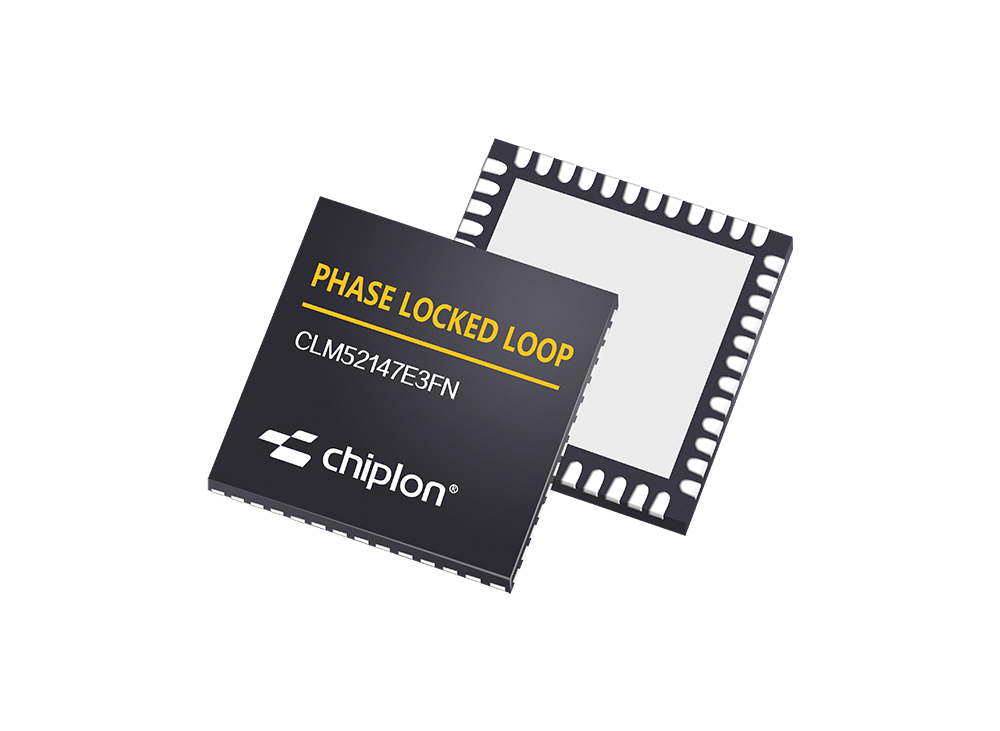
CLM52147 is a high-performance PCIe device generated synchronous clock generator launched by Chiplon, which can provide nine output PCIe clocks sourced from 25 MHz crystals or clock inputs. The clock output complies with the PCIe Gen 1, Gen 2, Gen 3, Gen 3 SRNS, and Gen 4 universal clock specifications. The device has six hardware output enable control pins for enabling and disabling differential outputs. In addition, it supports programming and configuring output parameters through the I ² C/SMBus interface, and frequency hopping control pins for reducing electromagnetic interference are also available. Adopting push-pull HCSL output buffer technology and fully integrating terminal resistors, miniaturization, and low power consumption characteristics, it becomes an ideal clock solution for embedded applications. The product can directly pin to pin replace similar international products without the need to change the circuit board or system software, achieving complete compatibility and replacement. Chiplon Microelectronics has developed its own testing plan to ensure that the factory products meet or even exceed the original specifications, supporting industrial grade working temperatures (-40 ℃~85 ℃). Competing product: SI52147-A01AGM
PCIe clock output, supporting Gen1/2/3
1 input, generating 9 HCSL differential outputs
Maximum output frequency 100MHz, operating voltage 3.3V
Support spread spectrum, I ² C programming, and integrated terminal resistors
Supports Serial ATA (SATA)
Compatible with differential output
No terminal resistor required
All clock output enable pins
Expand enable pins
25 MHz crystal input or clock input
Enable through pins or I ² C interface
Can effectively reduce electromagnetic interference (EMI) in the system
Package: QFN-48 (6x6)
Network Attached Storage
Multifunction Printer
Wireless Access Point
Server
